HDI PCB is frequently found in mobile phones, touch-screen devices,
laptop computers, digital cameras, 4G network communications, also
prominently featured in medical devices.
Advantages of HDI PCB
The most common reason for using HDI technology is a significant
increase in packaging density. The space obtained by finer track
structures is available for components. Besides, overall space
requirements are reduced will result in smaller board sizes and
fewer layers.
Usually FPGA or BGA are available with 1mm or less spacing. HDI
technology makes routing and connection easy, especially when
routing between pins.
Function improved by HDI PCB:
1.Denser trace routing
2.More stable power
3.Reduce interference inductance and capacitance effects
4.Improve signal integrity in high-speed design
Accelerate Development with HDI Printed Circuit Boards
1.Easier to place SMD components
2.Faster routing
3.Reduce frequent relocation of components
4.More component space (also by Via-in-Pad)
Feature | Capability |
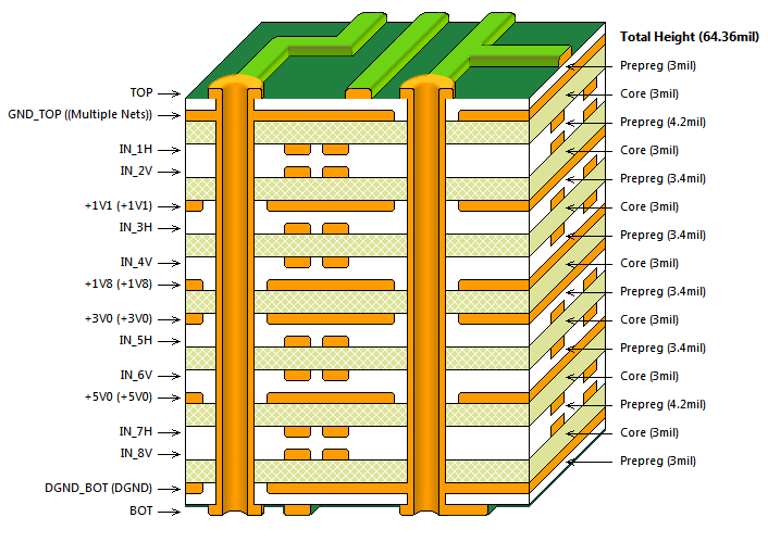
Number of Layers | 4-30 layer |
Quality Grade | IPC 6012 Class 2,IPC 6012 Class 3 |
Material | Tg 140°C FR4,Tg 150°C FR4,Tg 170°C FR4 ,Special material |
Thickness | 0.4-6.0mm |
Min Track/Spacing | 2-8mil |
Min Hole Size | 0.15mm-0.3mm |
Solder Mask | Green, Red, Yellow, Blue, White, Black, Purple, Matte Black, Matte
green |
Silkscreen | White, Black,Yellow,Blue |
Surface Finish | Immersion gold,OSP,Hard gold,Immersion Silver |
Finished Copper | 0.5-13oz |
Build time | 5-10 days |
Lead tim | 2-3 days |
The digital world is getting complex hour by hour whereas the
hardware associated with it is getting drastically smaller. The
advantages of HDI PCBs are numerous, starting with more
interconnections in smaller areas. This results in the
miniaturization of boards that can be used in many applications.
Your computers are no longer heavy. They are sleek and sexy. You
can work on your laptop and keep your business running while you
board a flight. You can also watch your favorite action movie on
your smartphone, some of which are way powerful than your laptops.
Or you can just plug in your wireless headphones and get into the
groove. Mankind is fond of electronics and it has become a part of
our lives. In this era, all the electronic devices are designed for
portability. Electronic devices are being designed for human
convenience. All this was possible because of the miniaturization
of the components and PCBs inside the electronic devices.
The PCB industry plays a prominent role in the development of all
the electronic gadgets. Let it be a pacemaker in someone’s chest or
the motherboard in a programmer’s workstation, PCB made it possible
for creating crucial electronic devices.
As the size of the components shrinks, printed circuit board
manufacturers adapted to the changing trends. This led to the birth
of HDI design. This has made PCBs smaller, denser with higher
component count, and faster.


